Value Stream Defect Generation and Detection

The quality level seen by the customer of our value stream is one of the most critical process metrics.
This quality level is the result of all the defects generated by the different process steps as well as those coming from the parts suppliers.
Ideally defects should not be produced in the first place. Unfortunately the state of the art, in many technologies, is still not there.
Therefore, on the mean time, we need process tests and controls to catch and correct defects as soon as they are produced.
In our Value Stream Map we focus on process flow but this flow is very much affected by quality.
It is important to find out where in the process each type of defect is generated and where in the process it will be detected to make sure it doesn’t find its way to the customer.

Control Plan
The Control plan defines all the controls, visual, test, etc., installed along the value stream in order to catch the defects as soon as they are produced in order to correct them and give immediate feedback to the step producing them.
These controls have a cost both in terms of manpower and flow drop so they should be minimized and installed just where and when they are required.
As the process is improved, by solving the root cause of the defects, controls can be removed or installed somewhere else.
The control plan is, therefore, a living document.
Electronic Board Assembly Process
Download this Excel simulator DPUdpmo.xls from OneDrive to your PC.
In this model we are simulating a simplified VSM of an electronic board assembly and test process:

Defect contributors are defective components coming from suppliers and defects from the 4 process steps:
- SMT (Surface Mount Technology) automatic component placement
- Reflow solder of these components
- Manual PTH (Pin Thru Hole) component insertion
- Wave soldering of PTH components.
- Several visual inspections along the process
- ICT (In-Circuit Test) at the end of the assembly process
- Final Functional test.
Defect Generation
“Defects per unit” (DPU) is the metric that interests the customer but it’s not very practical as a process metric because we are typically producing products with very different levels of complexity: some boards may have just 5 components and others 500.
“Defects Per Million Opportunities” (DPMO) is a useful process metric that is independent of the product complexity. This metric will allow us, for instance, to know if our soldering process is improving or getting worse with independence of the complexity of the products we are soldering.

In this example we have one defective component in 3 boards the average DPU = 1/3 = 0.33 (defects per board)
When we measure in DPMO we must define the OFEs (Opportunities For Error) of the process we are dealing with:
If our wave solder DPMO =500 this means that out of every million solder joints 500 will be defective on average.
When we measure in DPMO we must define the OFEs (Opportunities For Error) of the process we are dealing with:
- Component placement process: OFEs = Number of components placed
- Soldering process: OFEs = Number of solder joints soldered
If our wave solder DPMO =500 this means that out of every million solder joints 500 will be defective on average.
In the previous example to calculate DPMO we compute the OFEs = 3 boards x 12 components = 36
Therefore
DPMO = (1 x 1,000,000) / 36 = 27,777 defective components for every million placed.
State of the Art DPMO
Each type of process has a "State of the Art" DPMO that is the best DPMO being achieved in the industry in that process.This can vary widely from a DPMO of 10 in a highly automated robust process to a DPMO of 5000 in a manual process highly dependent on an "artist" skill.
For this reason DPMO values can not be compounded from different processes (with different OFEs) to obtain an overall DPMO.
DPMO is only useful to the process owner to know if the process is improving or to compare with similar processes. This metric has no interest for the customer.
In our Electronic Assembly example we have 500 SMT components and 100 PTH therefore these are the corresponding OFEs for the placement and insertion operations. Total components used per board is therefore 600.

The 500 SMT components have a total of 1500 solder joints, therefore these are the reflow solder OFEs.
The 100 PTH components have a total of 300 solder joints (wave solder OFEs).
Process DPMOs define the quality of our different process steps and the OFEs are specific for each product type.
In our Electronic Assembly example we have 500 SMT components and 100 PTH therefore these are the corresponding OFEs for the placement and insertion operations. Total components used per board is therefore 600.
The 500 SMT components have a total of 1500 solder joints, therefore these are the reflow solder OFEs.
The 100 PTH components have a total of 300 solder joints (wave solder OFEs).
Process DPMOs define the quality of our different process steps and the OFEs are specific for each product type.
The DPMO values for each process step are obtained from historical data of this process. There could be large differences between different board types depending on the mix of large and small components in the board.
On each step we can estimate the expected defects per unit:
Since the types of defects contributed by the 5 different sources are independent, the total number of defects produced will be sum of each defect contribution:
On each step we can estimate the expected defects per unit:
DPU = DPMO x OFE / 1,000,000
Since the types of defects contributed by the 5 different sources are independent, the total number of defects produced will be sum of each defect contribution:
Total DPU is the sum of all DPUs
DPU and Yield
Process Yield is the proportion of defect free units when tested. If defects are independent DPU follows a Poisson distribution so Yield and DPU are related by:
Yield = exp(-DPU)

For instance an average of 1 defect per unit will still produce exp(-1) = 0.37 that is 37% defect free units (there will be units with more than one defect)
Total DPU is therefore the sum of DPUs while the total Yield is the product of yields.
 |
Defect Detection

Visual inspection is performed as close as possible to the step generating the defect and the defects detected are typically corrected on the spot. The problem is that it is very inefficient: it can only catch 60% of the defects. In this example this means that out of the total 0.38 DPUs only 0.228 will be caught and corrected, therefore 0.152 will escape this control.
Visual inspection operators, if they are qualified to do rework they will report the defect and correct it, otherwise the board needs to be taken out of the stream and sent for rework.
In this example we notice that 20% of the inspected boards need to be reworked so we can calculate the workload required to do this.
We must also be aware that the 20% reworked boards will join the stream again and be reinspected so this means that the visual inspection workload will be for 120% of the boards built. See Test/ Repair Loop
ICT uses a bed of nails to contact many points in the board and is able to test the functionality of some components. If the test coverage is 80%, 0.122 DPU will be caught in ICT and corrected and therefore 0.03 will escape.
Finally the functional test has a high test coverage but the test is not able to pinpoint where the defect is, therefore faulty boards need to be analyzed and repaired by an expert through a lengthy process.
In the case of ICT and functional test 14% of boards will require rework and this may require a higher level of skills and it will take longer to identify and correct these defects. Again, reworked boards will need to be retested adding to the test workload.
Process Improvement
At the end of this process we have 1,520 faulty boards out of every million going to the customer.This is obviously unacceptable so we can start looking at the main contributors to defects and the main escapes of our detection and correction.
We can look at different improvement alternatives with this simulator and estimate the effect on the final ppms going to the customer.
PTH insertion, being a manual operation, is the main contributor to defects. We can look at ways to add some Poka-Yokes (defect proof devices) or look at ways to automate. Suppose we are able the reduce the PTH insertion DPMO from 1500 to 500 the result would be a reduction of output to 1,120 ppm.
If we can further improve visual inspection coverage by automation to 80% them it would go down to 560 ppm.
If we redesign the board to eliminate all PTH components and convert them to SMT we would further reduce it to 384 ppm.

In this simulator Process DPMOs come from measuring our current processes. Theoretically they should be Product independent but in actual fact they are not: some designs produce more manufacturing defects than others and the process parameters for some products may not be optimized.
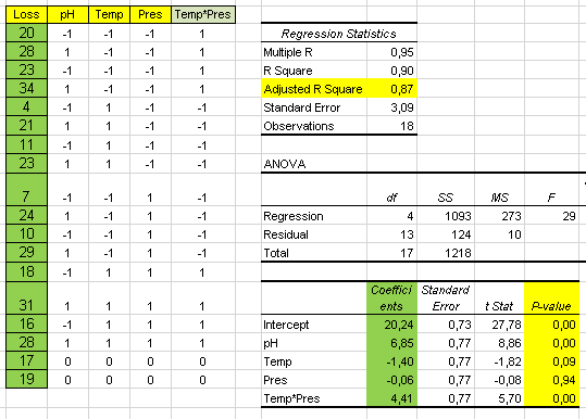
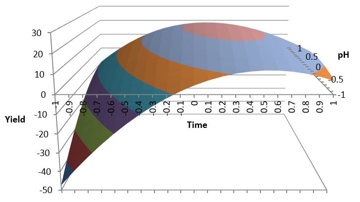
When we try to reduce wave solder defects we realize that there is, typically, a mix of component sizes on the board. When the board goes through the wave solder (typically at 250º C) small components reach this temperature immediately but large components take longer. This means that some components may be over heated and others under heated causing defects. We can find the optimal process parameters (solder temperature and conveyor speed) with Design of Experiments for each type of board.
Inspection Coverage Improvement
Visual inspection has typically a low coverage, especially with complex products.
As an example try to find a missing component in this board:

A simple "Comparascope " has been used to detect these defects by presenting a picture of the suspect board followed by a picture of a good board alternating between the two:

You can easily see component C48 flickering.
This simple aid could allow us to increase the visual inspection coverage.
Supposing that we are able to increase our inspection coverage in our original example from 60% to 80% we can see the impact to the customer with our simulator:

We can see a defect rate decrease from the original 1,520 ppm to 760.
Our improvement actions are mainly directed to avoiding defects from being produced on the first place, but we can work in parallel on the improvement of the defect detection process.
Conclusions
- Understanding the different mechanisms in our value stream which cause defects is essential to eliminate the root cause or, at least, detect and correct them upstream.
- This simulation helps us focus on the main contributors of defects in order to give feedback to those producing them
- The overall process control plan defines the controls and tests along the value stream in order to detect and correct defects as soon as they occur
- The control plan needs to be updated after each improvement in order to optimize resources
- Analysis of defect escapes from our tests detected further along the process should help to increase test coverage of previous steps and get to the root cause of defect generation.
- DPMO is a useful metric for process steps and simulation allows us to estimate the DPU the customer will see.
- State of the art DPMOs are very different for different processes and products.
- DPMOs from different processes, therefore, can not be compounded to obtain an overall DPMO.
- DPMO is for those working in a particular process, not for the customer.
- Yield and coverage measure the effectiveness of tests and controls in our control plan.

Comments
Post a Comment